- 您现在的位置:买卖IC网 > Sheet目录3855 > PIC16LC711-04/SS (Microchip Technology)IC MCU OTP 1KX14 A/D 20SSOP
111
7593L–AVR–09/12
AT90USB64/128
Bits 1:0 – WGM01:0: Waveform Generation Mode
Combined with the WGM02 bit found in the TCCR0B Register, these bits control the counting
sequence of the counter, the source for maximum (TOP) counter value, and what type of wave-
form generation to be used, see Table 14-7. Modes of operation supported by the Timer/Counter
unit are: Normal mode (counter), Clear Timer on Compare Match (CTC) mode, and two types of
Pulse Width Modulation (PWM) modes (see “Modes of operation” on page 103).
Notes:
1. MAX
= 0xFF
2. BOTTOM = 0x00
14.8.2
TCCR0B – Timer/Counter Control Register B
Bit 7 – FOC0A: Force Output Compare A
The FOC0A bit is only active when the WGM bits specify a non-PWM mode.
However, for ensuring compatibility with future devices, this bit must be set to zero when
TCCR0B is written when operating in PWM mode. When writing a logical one to the FOC0A bit,
an immediate Compare Match is forced on the Waveform Generation unit. The OC0A output is
changed according to its COM0A1:0 bits setting. Note that the FOC0A bit is implemented as a
strobe. Therefore it is the value present in the COM0A1:0 bits that determines the effect of the
forced compare.
A FOC0A strobe will not generate any interrupt, nor will it clear the timer in CTC mode using
OCR0A as TOP.
The FOC0A bit is always read as zero.
Bit 6 – FOC0B: Force Output Compare B
The FOC0B bit is only active when the WGM bits specify a non-PWM mode.
However, for ensuring compatibility with future devices, this bit must be set to zero when
TCCR0B is written when operating in PWM mode. When writing a logical one to the FOC0B bit,
an immediate Compare Match is forced on the Waveform Generation unit. The OC0B output is
changed according to its COM0B1:0 bits setting. Note that the FOC0B bit is implemented as a
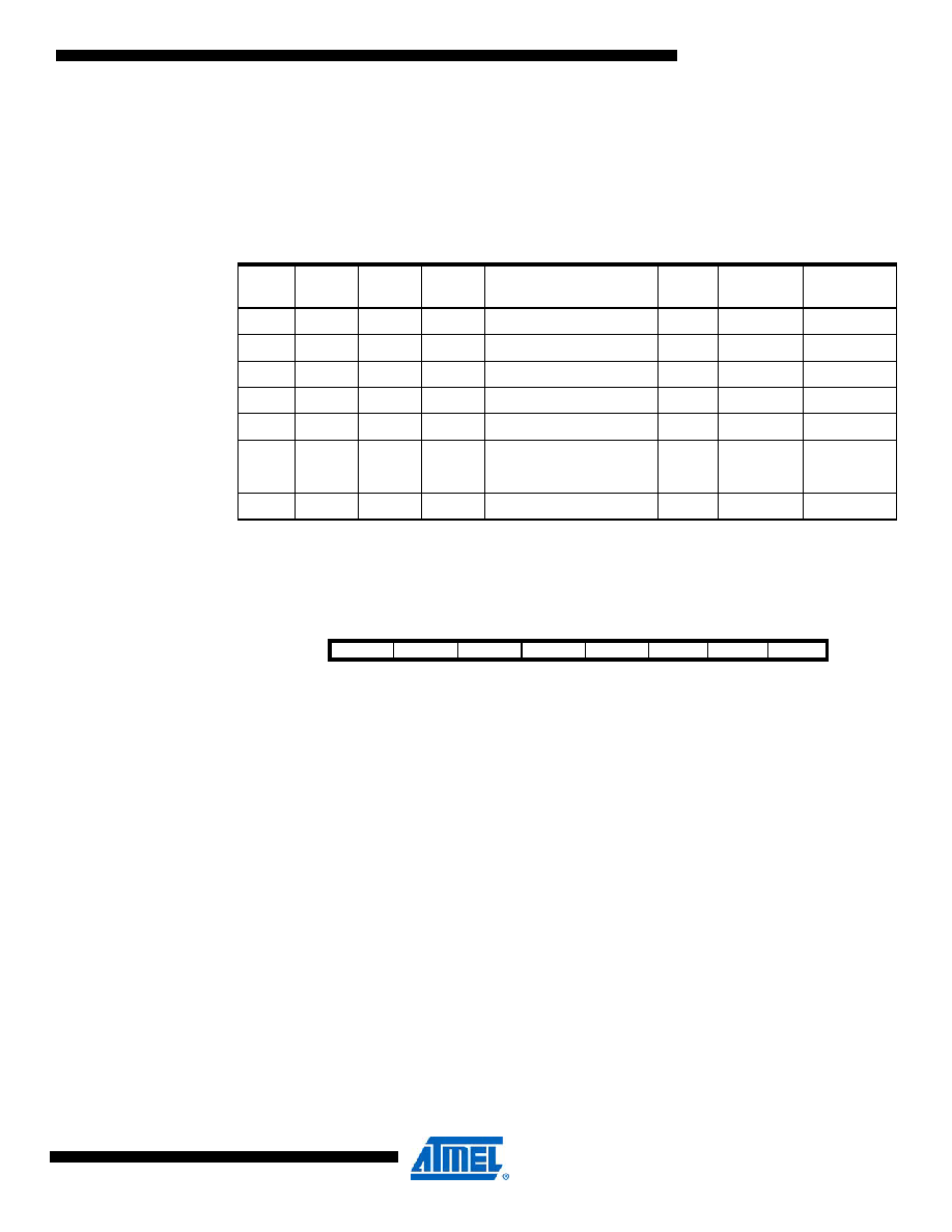
Table 14-7.
Waveform Generation Mode bit description.
Mode
WGM2
WGM1
WGM0
Timer/Counter mode of
operation
TOP
Update of
OCRx at
TOV flag
set on
0
Normal
0xFF
Immediate
MAX
1
0
1
PWM, phase correct
0xFF
TOP
BOTTOM
2
0
1
0
CTC
OCRA
Immediate
MAX
3
0
1
Fast PWM
0xFF
TOP
MAX
4
1
0
Reserved
–
5
1
0
1
PWM, phase correct
OCRA
TOP
BOTTOM
6
1
0
Reserved
–
7
1
Fast PWM
OCRA
TOP
Bit
7
6
543
2
1
0
FOC0A
FOC0B
–
WGM02
CS02
CS01
CS00
TCCR0B
Read/write
W
R
R/W
Initial value
0
发布紧急采购,3分钟左右您将得到回复。
相关PDF资料
PIC18F65K22-I/MRRSL
MCU PIC 32K FLASH MEM XLP 64QFN
PIC16LF87-I/SS
IC MCU FLASH 4KX14 EEPROM 20SSOP
PIC16C62B-20/SS
IC MCU OTP 2KX14 PWM 28SSOP
PIC16LC711-04I/SO
IC MCU OTP 1KX14 A/D 18SOIC
PIC18F66J90-I/PT
IC PIC MCU FLASH 64KB 64-TQFP
ATMEGA32L-8AC
IC AVR MCU 32K LV 8MHZ COM44TQFP
DSPIC30F2012-30I/SP
IC DSPIC MCU/DSP 12K 28DIP
PIC18LF2321-I/ML
IC PIC MCU FLASH 4KX16 28QFN
相关代理商/技术参数
PIC16LC711-04E/P
功能描述:8位微控制器 -MCU 1.75KB 68 RAM 13 I/O RoHS:否 制造商:Silicon Labs 核心:8051 处理器系列:C8051F39x 数据总线宽度:8 bit 最大时钟频率:50 MHz 程序存储器大小:16 KB 数据 RAM 大小:1 KB 片上 ADC:Yes 工作电源电压:1.8 V to 3.6 V 工作温度范围:- 40 C to + 105 C 封装 / 箱体:QFN-20 安装风格:SMD/SMT
PIC16LC711-04E/SO
功能描述:8位微控制器 -MCU 1.75KB 68 RAM 13 I/O RoHS:否 制造商:Silicon Labs 核心:8051 处理器系列:C8051F39x 数据总线宽度:8 bit 最大时钟频率:50 MHz 程序存储器大小:16 KB 数据 RAM 大小:1 KB 片上 ADC:Yes 工作电源电压:1.8 V to 3.6 V 工作温度范围:- 40 C to + 105 C 封装 / 箱体:QFN-20 安装风格:SMD/SMT
PIC16LC711-04E/SS
功能描述:8位微控制器 -MCU 1.75KB 68 RAM 13 I/O RoHS:否 制造商:Silicon Labs 核心:8051 处理器系列:C8051F39x 数据总线宽度:8 bit 最大时钟频率:50 MHz 程序存储器大小:16 KB 数据 RAM 大小:1 KB 片上 ADC:Yes 工作电源电压:1.8 V to 3.6 V 工作温度范围:- 40 C to + 105 C 封装 / 箱体:QFN-20 安装风格:SMD/SMT
PIC16LC711-04I/P
功能描述:8位微控制器 -MCU 1.75KB 68 RAM 13 I/O RoHS:否 制造商:Silicon Labs 核心:8051 处理器系列:C8051F39x 数据总线宽度:8 bit 最大时钟频率:50 MHz 程序存储器大小:16 KB 数据 RAM 大小:1 KB 片上 ADC:Yes 工作电源电压:1.8 V to 3.6 V 工作温度范围:- 40 C to + 105 C 封装 / 箱体:QFN-20 安装风格:SMD/SMT
PIC16LC711-04I/P
制造商:Microchip Technology Inc 功能描述:IC 8BIT CMOS MCU 16LC711 DIP18
PIC16LC711-04I/SO
功能描述:8位微控制器 -MCU 1.75KB 68 RAM 13 I/O RoHS:否 制造商:Silicon Labs 核心:8051 处理器系列:C8051F39x 数据总线宽度:8 bit 最大时钟频率:50 MHz 程序存储器大小:16 KB 数据 RAM 大小:1 KB 片上 ADC:Yes 工作电源电压:1.8 V to 3.6 V 工作温度范围:- 40 C to + 105 C 封装 / 箱体:QFN-20 安装风格:SMD/SMT
PIC16LC711-04I/SO
制造商:Microchip Technology Inc 功能描述:8BIT CMOS MCU SMD 16LC711 SOIC18
PIC16LC711-04I/SS
功能描述:8位微控制器 -MCU 1.75KB 68 RAM 13 I/O RoHS:否 制造商:Silicon Labs 核心:8051 处理器系列:C8051F39x 数据总线宽度:8 bit 最大时钟频率:50 MHz 程序存储器大小:16 KB 数据 RAM 大小:1 KB 片上 ADC:Yes 工作电源电压:1.8 V to 3.6 V 工作温度范围:- 40 C to + 105 C 封装 / 箱体:QFN-20 安装风格:SMD/SMT